We are continuously receiving many orders and inquiries from semiconductor manufacturers. The following applications are the examples we are collecting from our customers. Let us introduce how our indicators can support them. We would like you to know how NiGK’s products are used in this growing field. NiGK hopes this information could be any help for your business.
UV irradiation management by UV Label
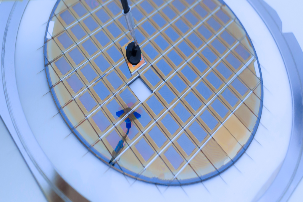
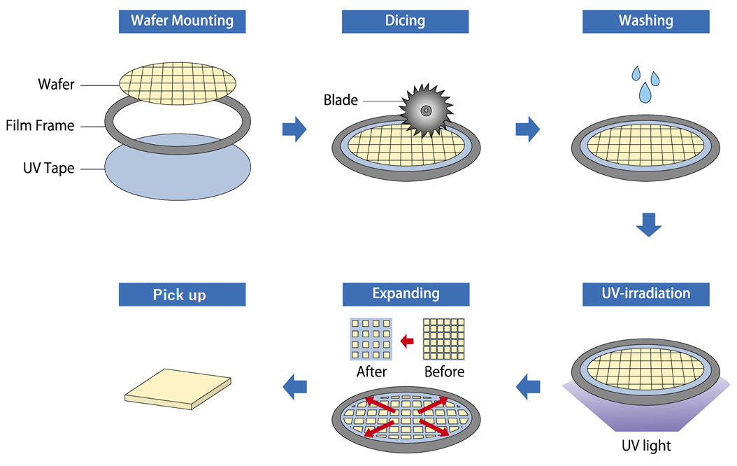
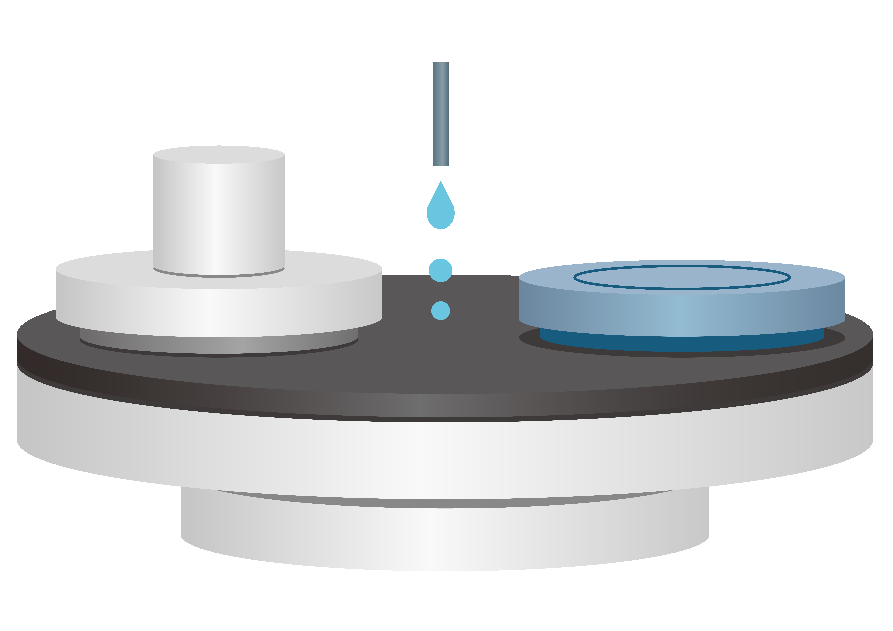
Dicing process
Before dicing (the process to separate dies from silicon wafer) , silicon wafers are typically mounted on dicing tape which the adhesive bond is broken by UV exposure. UV labels can check if the UV light is working correctly.
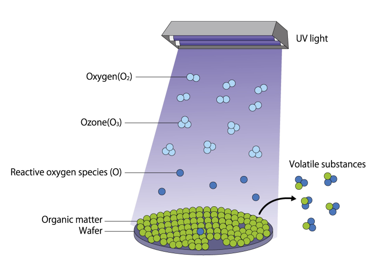
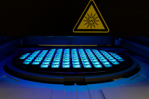
UV-Ozone cleaning process
UV irradiation generates ozone, which removes organic matter from the wafer surface. UV labels can be used to check if UV-Ozone Cleaners are working correctly.
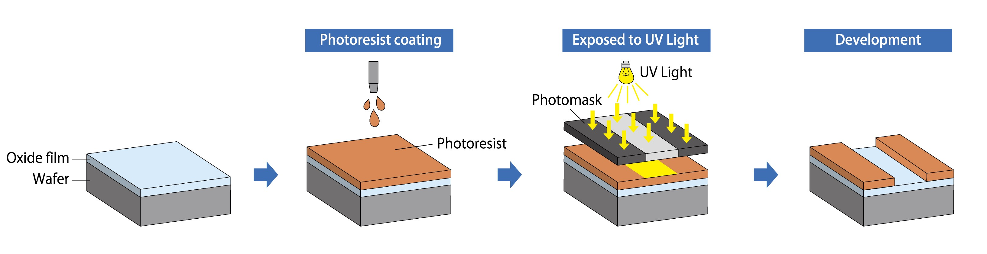
Photoresist Removal
Photoresist Removal is a process that removes photoresist from a silicon wafer. Photoresist melts when exposed to light and this makes it possible to create prominences and depressions. This allows for certain patterns to be created. UV labels provide a solution for checking the irradiation distribution and intensity of the UV irradiation light source for Photoresist Removal.
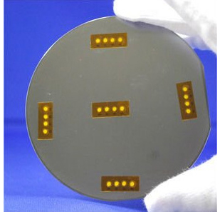
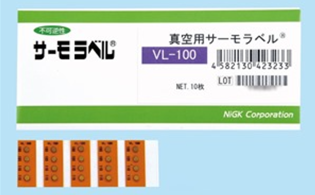
Vacuum condition makes easy to control chemical reactions and helps keeping the manufacturing space clean. If you attach the temperature indicators for vacuums (VL series) on a wafer, you can check the temperature easily even under the vacuum condition.
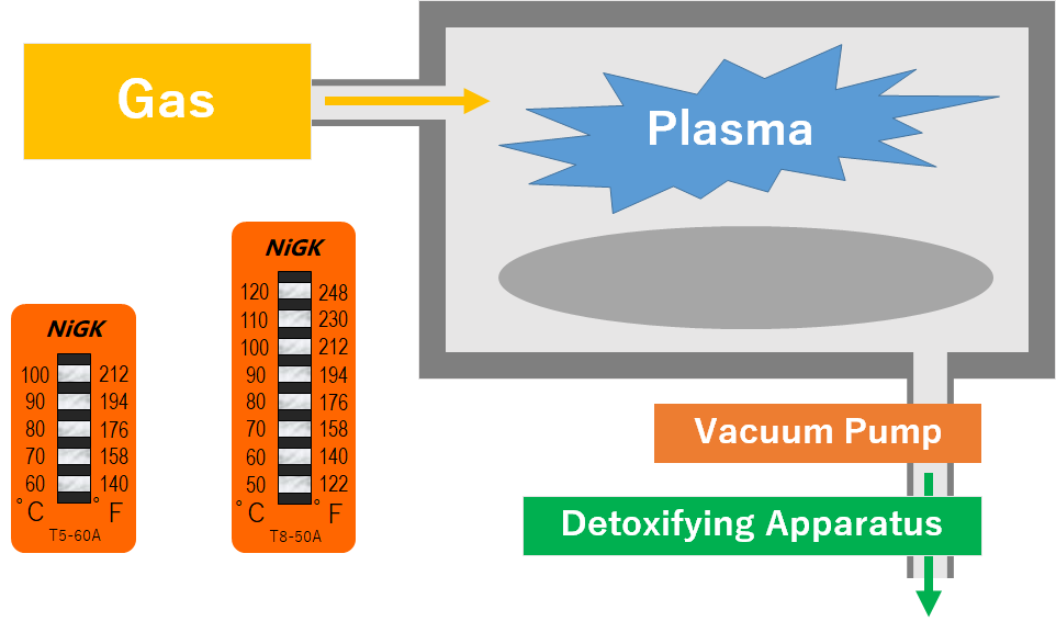
You can use temperature indicators in exhaust emission control system
Many kinds of chemical gases are used and emitted during the manufacturing process of semiconductors. Temperature labels also can be used in a fan motor of an exhaust emission control system to check abnormal heat.
An image of exhaust emission control system
A part of motor of exhaust emission control system
For checking temperature in Chemical-mechanical polishing (CMP) process
Semiconductor wafer is polished to smooth the surface in Chemical-mechanical polishing (CMP) process. During this process, heat is generated due to friction between the surface of the wafer and the polishing pad. Our temperature indicators are able to check the over heat of such narrow spaces and rotating objects to prevent unexpected damages.
We use cookies on our website to give you the most relevant experience by remembering your preferences and repeat visits. By clicking “Accept”, you consent to the use of ALL the cookies.
This website uses cookies to improve your experience while you navigate through the website. Out of these, the cookies that are categorized as necessary are stored on your browser as they are essential for the working of basic functionalities of the website. We also use third-party cookies that help us analyze and understand how you use this website. These cookies will be stored in your browser only with your consent. You also have the option to opt-out of these cookies. But opting out of some of these cookies may affect your browsing experience.
Necessary cookies are absolutely essential for the website to function properly. These cookies ensure basic functionalities and security features of the website, anonymously.
Cookie
Duration
Description
cookielawinfo-checkbox-analytics
11 months
This cookie is set by GDPR Cookie Consent plugin. The cookie is used to store the user consent for the cookies in the category "Analytics".
cookielawinfo-checkbox-functional
11 months
The cookie is set by GDPR cookie consent to record the user consent for the cookies in the category "Functional".
cookielawinfo-checkbox-necessary
11 months
This cookie is set by GDPR Cookie Consent plugin. The cookies is used to store the user consent for the cookies in the category "Necessary".
cookielawinfo-checkbox-others
11 months
This cookie is set by GDPR Cookie Consent plugin. The cookie is used to store the user consent for the cookies in the category "Other.
cookielawinfo-checkbox-performance
11 months
This cookie is set by GDPR Cookie Consent plugin. The cookie is used to store the user consent for the cookies in the category "Performance".
viewed_cookie_policy
11 months
The cookie is set by the GDPR Cookie Consent plugin and is used to store whether or not user has consented to the use of cookies. It does not store any personal data.
Functional cookies help to perform certain functionalities like sharing the content of the website on social media platforms, collect feedbacks, and other third-party features.
Performance cookies are used to understand and analyze the key performance indexes of the website which helps in delivering a better user experience for the visitors.
Analytical cookies are used to understand how visitors interact with the website. These cookies help provide information on metrics the number of visitors, bounce rate, traffic source, etc.
Advertisement cookies are used to provide visitors with relevant ads and marketing campaigns. These cookies track visitors across websites and collect information to provide customized ads.